|
Master Member
  加入日期: Feb 2005
文章: 1,908
|
引用:
雙方目前40nm 良率不知多少? 縮小製程良率不高的話價格可是下不來的. |
||||||||
 2010-09-04, 03:44 PM
#21
2010-09-04, 03:44 PM
#21
|


|
|
Power Member
 加入日期: Feb 2001 您的住址: 台灣苗栗
文章: 573
|
引用:
GTS450 GPU3 PPD測試:  |
|||
|
2010-09-17, 02:53 PM
#22
|
|
|
*停權中*
加入日期: Aug 2010
文章: 28
|
引用:
電源廠商:「我們準備好了」 巨大散熱器廠商:「我們準備好了」 消費者:「  」 」 |
|
|
2010-09-17, 03:00 PM
#23
|
|
|
Elite Member
加入日期: Dec 2006 您的住址: Taipei
文章: 8,344
|
引用:
OC一般是在考慮範圍外, 除非一段時間驗證過幾乎每一片都可以穩定達成, 對隊友來說 才不會過度承諾而出手買了經過包裝的產品. 為了消弭參與者只為跑分而選卡的外界雜音, 目前贊助都以顯卡本身在市場表現優異為前提, 如果450可以爭氣平反, 我隨時都可以來幫他錦上添花. 一張2.5k應該沒有對手了吧~ 剛好適用還在使用PPD 3k附近的中階卡隊友玩玩. |
|
|
2010-09-17, 05:57 PM
#24
|
|
|
Major Member
加入日期: Jan 2005
文章: 244
|
GTS 450 如果在官方預設時脈(192sp,783Mhz)真能跑到F@H PPD 7700分的話,
我認為已經相當不錯了,此時顯卡耗電量應為106瓦。 和GTX 460在官方預設時脈(336sp,675Mhz)跑F@H PPD約8千多分、耗電量150瓦相比,感覺GTS 450跑F@H的效能真是非常之好。 但玩遊戲或其他應用就是GTX 460大勝了。 雖然可以把GTS 450的時脈給超到900Mhz以上,但我相信此時耗電量會很難看。 增加的效能%數比不上增加的用電量(電費)... . 此文章於 2010-09-17 07:03 PM 被 k7system 編輯. |
|
2010-09-17, 07:00 PM
#25
|
|
|
Golden Member
加入日期: Dec 2002
文章: 3,258
|
小弟整理一下TPU所測3D均耗,
GTS450 OC沒比5770多耗多少電, ASUS這塊3D預設電壓還蠻高的,高達1.28,公版為1.08 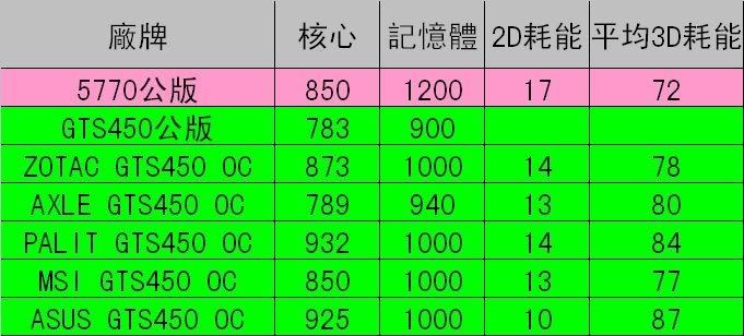 |
|
2010-09-22, 12:31 PM
#26
|
|
|
Advance Member
加入日期: Jan 2008
文章: 443
|
ASUS這張925MHz的GTS450電壓較高
最大耗電竟然直逼HD5850及GTX460 1GB 相當驚人...  以下是該站測Furmark Stability Test的最大耗電量: 112W: HD5770 1GB 148W: ASUS ENGTS450 TOP DirectCU 1GB (925MHz) 150W: HD5850 1GB 155W: GTX460 1GB |
|
2010-09-22, 05:53 PM
#27
|
|
|
Elite Member
加入日期: Dec 2006 您的住址: Taipei
文章: 8,344
|
引用:
以鐵匠九月份的VGAMASTER資料來看, PPD 似乎沒這麼優秀. 大約5500, GTS250的區間. |
|
|
2010-09-22, 06:57 PM
#28
|
|
|
Golden Member
加入日期: Dec 2002
文章: 3,258
|
引用:
所以看平均3D耗能或是看最高耗能就很關鍵, 一個相差十幾瓦,一個相差30~40瓦, 那一個較能反應真實? TPU所測有IDLE,AVERAGE,PEAK,MAXIMUM,BLU-RAY, 算是比較詳細,它的AVERAGE和別站有很大出入, 是否他站都抓PEAK或MAXIMUM,小弟也不太清楚... |
|
|
2010-09-22, 06:57 PM
#29
|
|
|
Golden Member
加入日期: Dec 2002
文章: 3,258
|
小弟整理了一些GTS450的耗能測試,
可以發現測試方法很多, 光軟體就有3DMARK,FURMARK,CRYSIS,Kombustor等, 大家或許可以參考一下, 但5系列節能設計較優是肯定的, NV 4系列的2D耗能也很優,但比5系列晚將近一年, 3D每瓦效能仍不及之,難怪眾人要撻伐了~~ I visited several websites and accomplished the following chart. 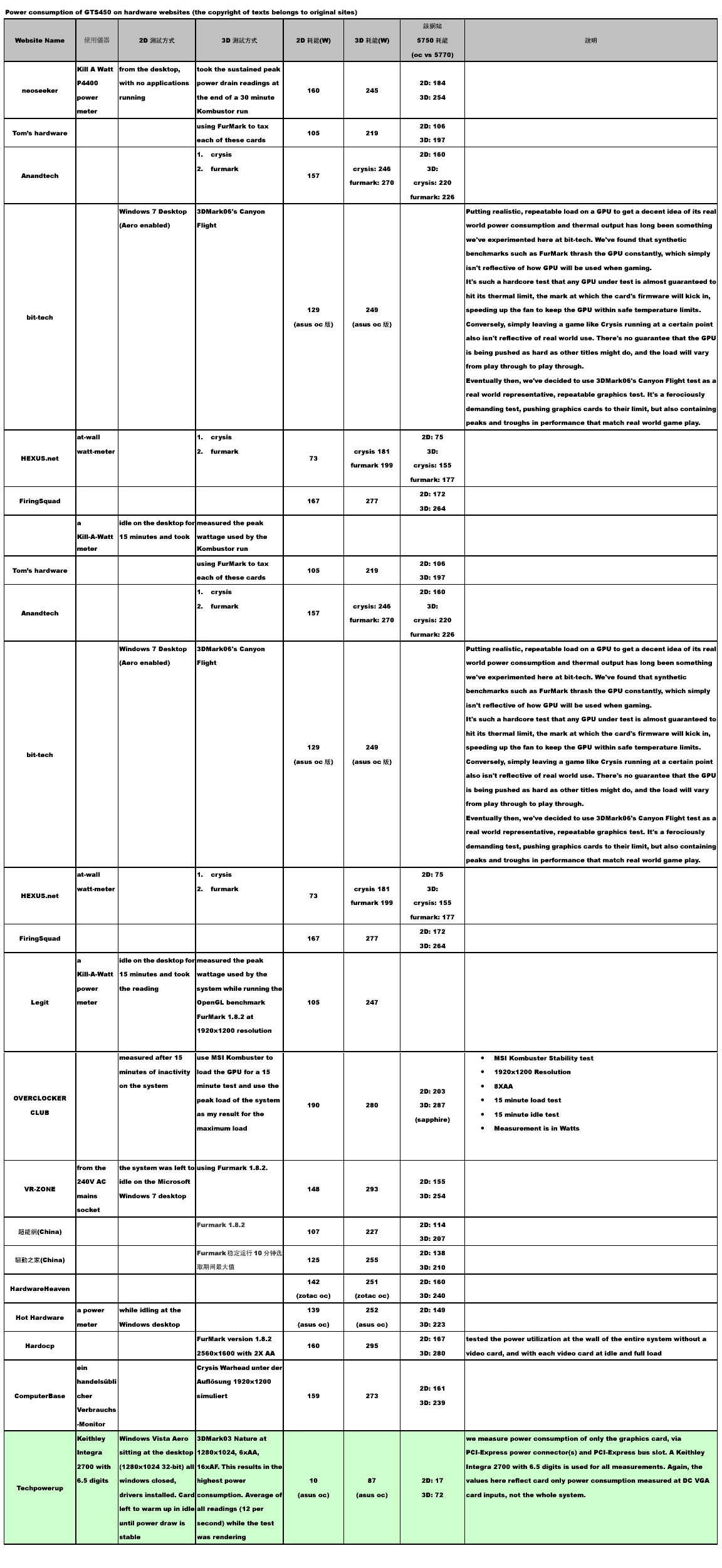 Every hardware website has its own way of measuring the power consumption of 3D cards, some websites give the details on how they get the “numbers”. Normally, 2D power consumption is measured while idling at desktop,no running programs at all. Under 3D, however, this gets a little complicated when every website uses different testing methods. For instance, some use 3dmark, some use furmark, and some use crysis, even MSI Kombustor is favored. This results in a big difference – websites using Kombustor show gts450 consumes less power than 5750, But websites using crysis or furmark show gts450 is more power hungry than 5750, I think under 3D 5750 is more power saving than gts450, still I have my doubts - First, Of what website do you think the most accurate while comparing to real 3D gaming conditions? Crysis? Heavily 3D stress reflects the real gaming conditions? Give your point to support your favored website. Second, TPU uses a unique way to get their numbers. They don’t test the whole system, but via PCI-Express power connector(s) and PCI-Express bus slot to gain the number, I think their “average 3D” is good although 3dmark03 is an antique, but for me “average number” is more convincing than peak readings. I give my vote to TPU, what is your point? |
|
2010-09-22, 07:04 PM
#30
|
|


