|
Silent Member
加入日期: Nov 2013
文章: 0
|
Samsung及Globalfoundries結盟宣告其14 FinFET製程首度採用3D電晶體架構,相較平面電晶體架構的20nm製程,速度可以提高20%,功耗則可降至35%,晶片尺寸也可減少約15%。早先言明,其採用20SoC製程的產品不擬在2014年上市的AMD率先呼應,成為首家採用14FF製程投片的業者,應用在內建CPU及GPU的行動裝置AP上。
 This offers a huge competitive threat to TSMC and provides an alternative to those companies who are looking to use leading-edge production. It’s a huge deal. - Jim McGregor at Tirias Research If Samsung and Globalfoundries bring the technology to the market in the time frame they are promising, it could put them at least six months ahead of the competition and tempt multiple chipmakers to give them orders. The partnership would also reduce the cost for chipmakers of alternating between the two suppliers, because products wouldn’t need to be redesigned, as they do now when companies switch. Now you have two well-respected organizations combining forces. For a customer, if you can truly have multiple sources, it changes everything. - Len Jelinek, an analyst at market-research firm IHS Inc. Samsung’s announcement […] is consistent with our Moore Stress thesis, and a big step forward to disrupt TSMC’s leading-edge business model by enabling a superior foundry process node with approximately a one-year lead over incumbent TSMC. Beyond enabling a stronger competitive position for Samsung in mobile devices, we continue to view TSMC disruption as a positive for MicronU, Sandisk, and Intel. Longer term we believe Samsung would be well positioned to take >50% share of the mobile device market, enabled in part by disruption of TSMC’s leading-edge foundry model this year. - Sundeep Bajikar with Jefferies & Co. We see the announcement as no surprise, given our having previously seen “2 new 193 nanometer scanners from ASML” installed at Global’s “Fab 8.” We believe this agreement is a landmark event that has the potential to massively disrupt the current state of the foundry industry, where TSMC has a near monopoly on the leading edge process nodes. The joint program offers a single process design kit (PDK) and volume manufacturing at four different fabs with identical processes: SAS (Austin), GF Fab 8 (Malta), S-1 (Korea) and S-3 (Korea). Multi-sourcing has become a huge issue with the foundries, particularly at the advanced process nodes. In 2012, Qualcomm suffered from severe shortages of 28nm Snapdragon devices that impacted their revenue when TSMC struggled with surging demand. In addition to the multi-sourcing benefit, we believe the Samsung/GF alliance will capture several major customers because of their technology lead with 14nm FinFET. Industry sources point to Samsung’s investment for over 3 years developing FinFET, giving them a sizeable lead on TSMC. The Samsung/GF FinFET is up to 15% smaller than TSMC’s process due to aggressive gate pitch and superior layout schemes. Additionally, the 14nm FinFETs offer a 20% improvement in performance and a 35% reduction in power compared to existing 20nm technology. We believe QCOM is also actively engaged with Samsung/GF at 14nm for next generation designs. While this may be surprising given the company’s long standing relationship with TSMC, we think there are several factors that swing in the Samsung/GF direction. The multi-sourcing arrangement alleviates QCOM’s concerns about having another severe product shortage like they did when TSMC ramped the 28nm node. The Samsung/GF FinFET technology lead and smaller transistors gives QCOM a time to market lead and superior integration capability versus their competitors. - Steve Mullane and Paul Peterson of BlueFin Research Partners Although Samsung, GF, IBM and STMicro have all been closely sharing R&D through the umbrella of Global Alliance, the Apr-17th joint press release takes this collaboration one step further and involves mass production of multiple versions of 14nm FinFET technology. This way, customers ]no longer would need to have different design rules nor mask sets and can send the same design for mass production[/COLOR […] We find the above news as negative for TSMC because: (1) one way or another, the above announcement is aimed at taking market share from TSMC, and [COLOR=Yellow]lower ASPs is the most effective way of doing it. (2) There are only a few customers that would be able to afford to migrate to 14nm; Apple/Qualcom (in AP), Nvidia/AMD (graphics), Altera/Xilinx (FPGA). Any market share loss at TSMC would lead to significant margin erosion since there may not be another customer with sufficient volume to fill the void left if any of these customers were to defect to Samsung/GF. (3) Samsung/GF can offer mass production of chips in US, closer to the above customers and also a positive factor for the likes of Apple/Qualcom as they can also claim enabling job creation at home. All TSMC’s fabs are in Taiwan. (4) TSMC’s 16nm FinFET Plus, which is closer to Samsung’s 14nm FinFET, won’t be available until 2H15 vs. Samsung/GF 14nm FinFET availability by YE14. - Mehdi Hosseini at Susquehanna Financial Group While TSMC will get the boost at 20-nanometer, it is likely to split those volumes across Samsung, Global Foundries, and TSMC at 14/16-nanometer and beyond, which will prove a negative for TSMC by the late 2015-to-early 2016 timeframe. TSMC's top- and bottom-line growth could come under pretty significant pressure as a result of a margin squeeze for leading-edge foundry capacity as well as share loss. - Ashraf Eassa, an independent research contrarian. 蘋果於2015年據聞已同時對台積的20奈米製程、以及16奈米FinFET+製程下單來看,台積於16奈米製程已有了大客戶的背書,取得了好的開始。關於三星與格羅方德結盟對台積可能形成的衝擊,市場似乎也無需太早、太過擔憂。 - moneydj@Apr 18'14 往昔TSMC以40/28nm領先策略在45/32nm節點勝出的優勢,或將在Samsung/Globalfoundries的技術與市場互補聯盟正事成軍後,產業態勢呈現可能的轉捩點,後者的14nm製程以領先競敵16nm一季度之姿投產,扭轉落後窘境。由於IDM霸主Intel已昭告,其跨足foundry領域不在爭霸,而是挹注未來先進製程研發經費,是故TSMC真正的對手明顯已是星格聯盟。雖然TSMC過半的市占優勢形同護城雷池,短期內依舊強不可撼,但星格聯盟在14nm製程量產上趕超TSMC,不啻一針提振士氣的強心劑。 |
|||||||
 2014-05-03, 09:07 PM
#261
2014-05-03, 09:07 PM
#261
|


|
|
Silent Member
加入日期: Nov 2013
文章: 0
|
引用:
比照TSMC最近兩季法說會訊息,所謂『16FF - 提速40% vs 20SoC』,應是16FF與16FF+的混淆。實際上可能是: 16FF - 提速27% vs 20SoC 16FF+ - 提速15%、節能30% vs 16FF 16FF+ - 提速40% vs 20SoC 目前28HPm打造的Snapdragon 801將可達2.5GHz(MSM8974ACv3),依照TSMC之效能指標,未來(以保守MSM8974VVv2的2.2GHz為推算基礎): 20SoC - 提速20% vs 28HPm → 2.2×1.2=2.64GHz 16FF - 提速27% vs 20SoC → 2.64×1.27=3.35GHz 16FF+ - 提速15%、節能30% vs 16FF → 3.35×1.15=3.86GHz 亦即,以16FF+打造之SoC,近4GHz速度是可期的。 PS: 不似28nm製程有28LP、28HPm、28HPC三種針對不同產品特性優化的細分,20SoC、16FF、16FF+均只有單一製程,目前仍不清楚其提速改善是否一體適用mobile SoC、CPU、GPU等不同訴求的處理器。缺乏foundry標準優化製程的便利,在遵循foundry設計準則的同時,預期fabless須倍加強化自身架構的優化與深化和foundry工程人員的互動。 類似TSMC的16FF、16FF+製程,Samsung/GF目前也有14LPE(Low Power Early)、14LPP(Low Power Plus)兩種。 16FF - 2014年1月完成製程認證,4月收到first tape-out。 16FF+ - 2014年9月預計完成製程認證。 14LPE - 2014年2月完成製程認證,2014年底投產。 14LPP - 2015年導入。 鷸蚌相爭,孰得利?Intel嗎?No!我只想賺點貼補家用的錢。 Whether Intel could lure Apple or Qualcomm if the current suppliers of those companies continue to run up against problems with FinFet?Questions about what such would look like, fears of 30%-40% gross margins play off against this year’s better than $3bn mobile loss. One would think an Apple/Qualcomm arrangement would cease Intel’s present mobile course, and eliminate this year’s $0.60 EPS hit. Intel’s wish is to fill its fabs at profit rates sufficient to fund process R&D while focusing on PC legacy and fending off ARM in Data Center. - Richard Whittington with Drexel Hamilton |
|||
|
2014-05-05, 11:10 AM
#262
|
|
|
*停權中*

加入日期: Oct 2003
文章: 472
|
頻率應該不會再上去了
桌機雖然也有4G但是問題不少 比較有可能的是同頻下效能加15% 這樣比較實惠 其實今年的旗艦機SONY已經推4K錄影了 CPU大概這樣就夠了,更省電會比較有吸引力 此文章於 2014-05-05 08:51 PM 被 teszd 編輯. |
|
2014-05-05, 08:50 PM
#263
|
|
|
Silent Member
加入日期: Nov 2013
文章: 0
|
引用:
是虎是豹,拉出來咬咬就知道!沉潛兩年,影武者Kabini/Temash退位,本尊Beema/Mullins現身。  AMD SoC diagram  AMD Mobility Roadmap  AMD以低功耗為訴求的微架構研發不及,為求2013年卡位,倉促以未完成品Jaguar急就章上場充數,一年後,完全體Puma+功成出關,力戰Intel低功耗版Haswell與Atom,其中Mullins SoC更是專對Tablet市場而來。 在已完成的Jaguar主架構上,AMD過去一年內最終成功成功建置入過去未完成的瞬間智慧超頻(Intelligent Boost)技術與PSP(Platform Security Processor)硬體保全功能,佐以更優化的28nm製程,精煉出Puma+微架構。 Puma+ is based on the same micro architecture as Jaguar, a 2-wide OoO design with the same number of execution units and data structures inside the chip. The memory interface remains unchanged as well at 64-bits wide. These new SoCs are still built on the same 28nm process as their predecessor. The process however has seen some improvements. Not only are both the CPU and GPU designs slightly better optimized for lower power operation, but both benefit from improvements to the manufacturing process resulting in substantial decreases in leakage current. 為求更低的功耗,Beema/Mullins毅然放棄前代對多種DRAM模組的支援彈性,加強限制,且依然未支援在手機蔚為主流的AP+DRAM的PoP封裝。 Beema and Mullins platforms now ship with more strict guidelines as to what sort of memory can be used on board and how traces must be routed. The result is a memory interface that shaves off more than 500mW when in this more strict, low power mode. OEMs looking to ship a design with socketed DRAM can still run the memory interface in a higher power mode to ensure memory compatibility. Beema/Mullins also show up to a 200mW reduction in power consumed by the display interface compared to Kabini/Temash. Beema and Mullins are definitely in a good place, however they still do consume more power at idle than the smartphone SoCs we typically find in iOS and Android tablets. 師法Intel作風(其實其他業者的Mobile SoC亦然),AMD現在也提供如汽車引擎般在短時間內提高轉速來換取更高扭力以加速的Turbo模式 - Intelligent Boost。 Beema and Mullins SoCs can take advantage of available thermal headroom to increase their maximum frequency for a limited period of time. Similar to what Intel discovered in architecting its Bay Trail silicon, the fact that in ultra portable form factors it would run into a chassis temperature limit before it ever reached the maximum operating temperature of its silicon, AMD hit significantly higher frequencies without a substantial architecture change or new process node by raising the max thermal operating point of the silicon. 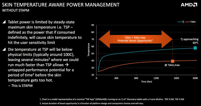 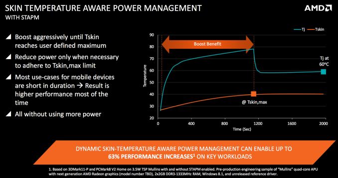 顧及機殼表面溫度影響所及的所用戶體驗,可耐熱至100°C的晶片核心,AMD在達60°C時便開始對CPU/GPU鎖頻。其實在100°C的物理極限內作短時間的超頻既不使機殼溫度長時間過度飆升,也不傷及SoC本身,何樂而不為?這就是STAPM(Skin Temperature Aware Power Management)節能技術。神奇之處是這項技術毋須系統廠在硬體上添加額外的溫測器。 What really matters isn’t if the silicon is running warm but rather if the chassis is running too warm. With Beema and Mullins, AMD increases the silicon temperature limit to around 100°C (still within physical limits) but instead relies on the surface temperature of the device to determine when to throttle back the CPU/GPU. In AMD’s own words, this allows the SoC to run at a much higher frequency for up to several minutes before having to scale back down. Without requiring any additional sensors or hardware from the OEM, what AMD does instead is gives the OEM tools to properly map SoC temperature to chassis skin temperature.   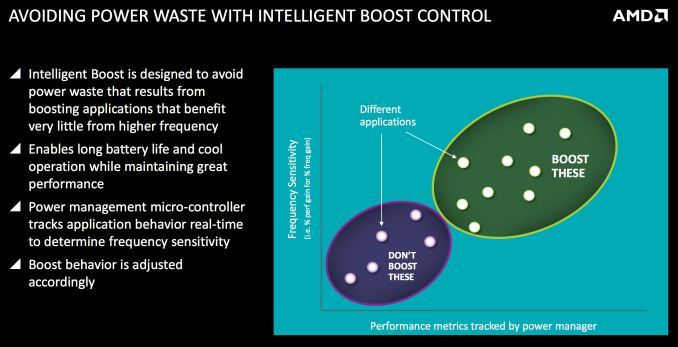 AMD宣稱,其Intelligent Boost可自行判斷超頻的時機,不浪費不必要的功耗。 The updated power management unit looks at the response to frequency scaling of a given workload and will only boost when the workload will actually benefit from being boosted. This evaluation happens at the hardware instruction level and not at the OS/software layer.  2012年向ARM授權Cortex-A5的AMD,雖然隔年便在其Kabini/Temash中植入,因為相關軟體未及時就緒而任其沉眠,直至今日終於有能力將其喚醒,抗衡Intel TXT(Trusted Execution Technology)。   叫板Bay Trail-T,Mullins效能來勢洶洶。  AMD處理器功耗遷移沿革  好戲在後頭,AMD技術水平向Intel靠攏,壓箱寶即將盡出,能一搏Intel嗎? |
|
|
2014-05-08, 06:15 PM
#264
|
|
|
Silent Member
加入日期: Dec 2013
文章: 0
|
之前看過一個數據 5W大概是平板與大手機的ㄧ個極限。
超過5W就要加散熱片(heat sink)了。 看來tablet market,AMD也許有機會進來play一下。 但是沒有wifi ,3G and LTE技術在手。怎麼強攻 Qualcomm,MTK 霸佔的mobile市場。 不過Ultra slim NB市場,搞不好可以捲起一些漣漪~ |
|
2014-05-08, 06:52 PM
#265
|
|
|
Silent Member
加入日期: Nov 2013
文章: 0
|
天橋把戲人人會?AMD Skybridge當讓你刮目相看!
 繼代號Seattle的64-bit八核ARM-A57微伺服器CPU,AMD的司馬昭之心終於纖毫畢露,ARM與X86的兩翼包抄策略正式進軍利基電算領域。 AMD is no longer married to x86 exclusively and by offering OEMs pin compatible x86/ARM solutions it gets to play in both markets, as well as benefit if one increases at the expense of the other.  前AMD大將Jim Keller跳槽Apple參與設計A4、A5後,於2012年回鍋AMD,經過兩年醞釀,首度揭開AMD秘密武器Skybridge的面紗。改弦易轍的AMD唯『利』是圖,迴避PC處理器的殺戮紅海,專注利基應用的嵌入式運算、高密度伺服器、半客製晶片。天橋專案將在2015年推出針腳相容,整合GCN繪圖核心的X86與ARM晶片(共用主機板),企圖在網通市場掃蕩MIPS跟PowerPC。此ARM晶片會用20nm打造,面向embedded與client市場,而非server(Seattle足矣),並首度支援Android。 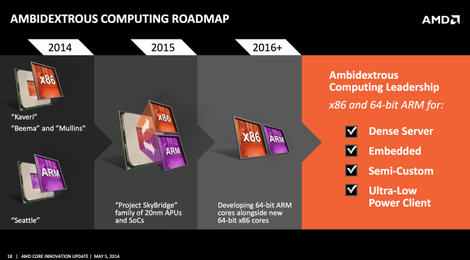 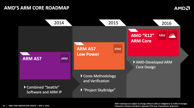 除了明年主打低功耗的Cortex-A57 CPU,相容ARMv8的AMD自主架構K12,或將強調效能,隨後在2016年問世,屆時應該是16/14FF製程。另外,更新一代的X86微架構研發也在進行中。 Server, embedded and semi-custom (offering just a CPU/GPU core with other IP) markets are obvious targets for K12.  在半客製晶片的新核心策略下,X86內核與ARM內核或將朝向模組化架構,便於與其他IP融合。 |
|
2014-05-08, 07:26 PM
#266
|
|
|
Silent Member
加入日期: Nov 2013
文章: 0
|
引用:
引用:
引用:
離首顆Cortex-A53處理器Snapdragon 410上市僅剩數月,在眾人引頸企盼下,ARM提供最新效能數據供大家一窺奧秘。  以瀏覽網頁之類的工作負載,同樣28nm製程之下(應是代表相同頻率下),CA53、CA57都能提供較現行CA7、CA15提升近50%的效能;而在新製程(20/16nm,應是代表時脈獲得提升)下,可再改善各約20%、40%。  微架構更優化的CA57在32-bit Geekbench跑分測試下,仍較同頻的CA15快約15%~30%。 |
|||
|
2014-05-08, 09:09 PM
#267
|
|
|
Silent Member
加入日期: Nov 2013
文章: 0
|
引用:
In our April 28th Apple Update, we noted that 20nm production levels at Samsung Austin were in the 3000-4000 wpm range. These volumes were sufficient to debug/improve their yields as they vied for second source position for the Apple designs. But our latest checks indicate a surprising twist to the 20nm development story. We are getting indications that Samsung Austin is planning to ramp their 20nm technology designs to 12,000 wpm by July, but the upside is for Qualcomm, not Apple. It is our understanding that Qualcomm is not happy with the 20nm development/yield progress at TSM and thus have been qualifying their latest technology node designs at Samsung. Obviously, the potential loss of business from Apple and Qualcomm would be bad news for TSM after recently losing the AMD GPU business. And while 20nm demand will continue to be strong for TSM, we expect Samsung to be a viable threat to TSM for the advanced process nodes going forward. - Steve Mullane and Paul Peterson of BlueFin Research Partners 就會搞我,佛也發火? 就在AMD與nVidia宣稱不擬在2014年轉進20nm製程的GPU之際,緊盯Samsung Autin Fab S2動態的藍鳍研調公司發現,S2擬將其20nm晶圓投入在七月前提高2~3倍至每月12000片,判斷是TSMC的新節點20SoC再現當年28nm導入初期的產能短缺現象,促使Qualcomm對Samsung追加訂單。 雖然Qualcomm今年的訂單大量仍在28nm,但年底的Snapdragon 808/810旗艦晶片仰賴20nm製程,不容有失;然在TSMC嬌客入門Apple入門之際,對其他現行客戶產生的排擠效應不無可能。不排除Qualcomm為避險而兩邊押寶,來個小心不蝕本的重覆下單,至少壓壓驚。 |
|
|
2014-05-09, 01:29 PM
#268
|
|
|
Silent Member
加入日期: Nov 2013
文章: 0
|
引用:
中國4G之戰,即將豬羊變色?Qcom大難臨頭?  業界傳出,MT6290數據晶片比預期提前,而且只花了一個月的時間,已完成了中移動TD-LTE入庫測試。 中國工信部壓寶TD-LTE,技術性拖延FDD-LTE的營運執照發放至五月,且初期僅開放20個城市;而中移動亦不再堅持五模AP單晶片,允許外加五模數據晶片的做法。MT6290有機會在第三季殺入4G戰場,對決Qcom。 TCL旗下Alcatel One Touch POP S7與LTE版的酷派大神均搭載MT6592/MT6290的雙晶片方案,之前均已公開展示。 |
|
|
2014-05-11, 10:09 PM
#269
|
|
|
Silent Member
加入日期: Dec 2013
文章: 0
|
引用:
AMD是標準的不怕神一樣的對手,只怕豬一樣的隊友。一般ODM,OEM通常不會把一軍拿去做AMD的東西。了不起是2-3軍去玩玩看,練練功。 而embedded 領域的東西客製化的層度很深,也不是只把Windows開起來就可以打進去的領域。AMD除了graphic比別人好,其他東西不一定能贏過其他的vendor。尤其客製化這一塊。 AMD 現在才開始玩Android,timing 也比別人慢了好幾拍。要走平板tablet的領域 只能期待Windows9能大發神威。不然以上的問題不解決。 只能在遊戲機逞逞威風,一些Digital TV與Casino gaming的應用也只能在旁邊流口水而已。 |
|
|
2014-05-12, 01:00 AM
#270
|
|


