|
Senior Member
 加入日期: Feb 2011
文章: 1,038
|
Radeon HD 7970正面照片、官方詳測放出
今日是Radeon HD 7970 NDA解禁前的最後一天,各路神仙又紛紛出馬各顯神通給大家放料來了:
首先還是國內論壇chiphell的爆料王bigpao007,為大家奉上了Radeon HD 7970的高清無碼正面大圖。這張樣卡據稱長度與Radeon HD 6990相當,此外作為為數不多的樣品自然產自原ATi的加拿大工廠。目前AMD隨卡提供的驅動8.940 RC2據稱還有不少問題,部分遊戲測試無法完成。 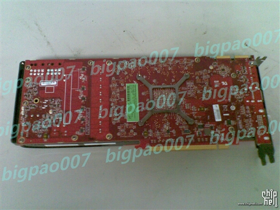 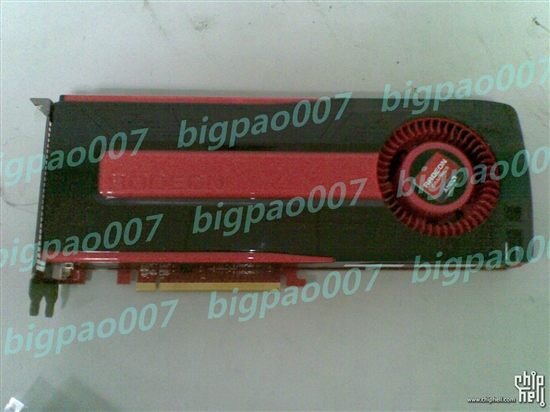 然後是國外論壇XtremeSystems放出了AMD官方幻燈片關於通用計算/HD3D的一部分,其中完整列出了支援AMD HD3D技術的所有遊戲,以及Radeon HD 7970對比Radeon HD 6970在通用計算方面提升的幅度 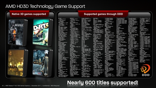 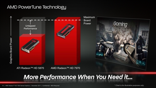  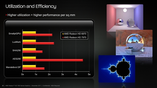 最後壓軸大戲是我們的“老朋友”土耳其DonanimHaber,完整列出了AMD官方提供的Radeon HD 7970、Radeon HD 6970和NVIDIA GeForce GTX 580 1.5GB版的性能對比測試資料,包括SLI、Crossfire以及7680*1600 Eyefinity變態解析度下的性能對比: 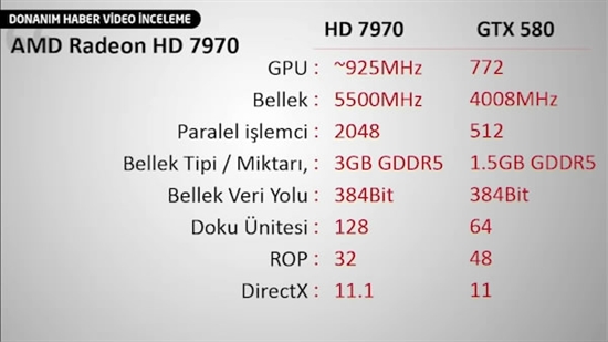 詳細測試頁面 http://news.mydrivers.com/1/212/212694_1.htm 來源: http://news.mydrivers.com/1/212/212694.htm |
|||||||
 2011-12-21, 04:47 PM
#1
2011-12-21, 04:47 PM
#1
|


|
|
Senior Member
加入日期: Jun 2003
文章: 1,366
|
雙PCIE 6-pin power connector
 看來耗電不會太高 |
||
|
2011-12-21, 05:14 PM
#2
|
|
|
Golden Member
加入日期: Jan 2006
文章: 2,552
|
真是萬年不變造型
 |
|
2011-12-21, 06:01 PM
#3
|
|
|
*停權中*
加入日期: Jun 2010 您的住址: 紐開普市
文章: 1,545
|
引用:
單核卡7970跟現在的雙核卡6990長度相當 那未來如果還要推出雙核卡7990 那卡是要長到哪去 |
|
|
2011-12-21, 06:11 PM
#4
|
|
|
*停權中*
加入日期: Dec 2006
文章: 2,931
|
引用:
這倒是出乎意料...原來不是說6+8嗎? |
|
|
2011-12-21, 06:21 PM
#5
|
|
|
Major Member
加入日期: Mar 2005
文章: 148
|
看起來從5系列開始 AMD中高階顯卡長得好像都一樣了
題外話 chiphell怎麼變國內了@@? 此文章於 2011-12-21 06:32 PM 被 mix947 編輯. |
|
2011-12-21, 06:30 PM
#6
|
|
|
Senior Member
加入日期: Dec 2004
文章: 1,001
|
卡變長了!?
 靠∼這樣cm690 II不就塞不進去了  |
|
2011-12-21, 06:38 PM
#7
|
|
|
Golden Member
加入日期: Dec 2002
文章: 3,258
|
http://www.techpowerup.com/157181/A...ured-Clear.html
sample有6+6pin,也有6+8pin Here is the first clear picture of Radeon HD 7970 engineering sample PCB. The final product will feature an all-black PCB color. The picture reveals the PCB to have provision for two 8-pin PCIe power connectors, though on this sample, there are two 6-pin connectors. We've seen other samples using 8 + 6 pin connector arrangements. Unlike earlier thought, the HD 7900 single-GPU reference board very much does use a digital-PWM power design. There appears to be CPL-made single-phase PWM chokes, and Volterra-made regulators. Not all power domains, though, seem to have digital-PWM. We can find a 5+1+1 phase VRM, with some miscellaneous analog power domains. The GPU package design is nothing like we've seen from AMD. It looks to be slightly larger than that of AMD Cayman. The die is oriented diagonally, with a sturdy brace around it reduce and stabilize the pressure applied by the cooling assembly. There are twelve memory chips around the GPU, as this chip features a 384-bit wide memory interface, to deliver nearly 50% higher memory bandwidth over the previous generation. The card features redundant BIOS, loaded into two separate EEPROM chips that can be toggled using a small 2-way switch located next to the Crossfire connectors. Display connectors include one DVI, one HDMI, and two mini-DP connectors. The second picture below reveals a curvy back-side of the cooling assembly. A nice aesthetic touch with zero function. 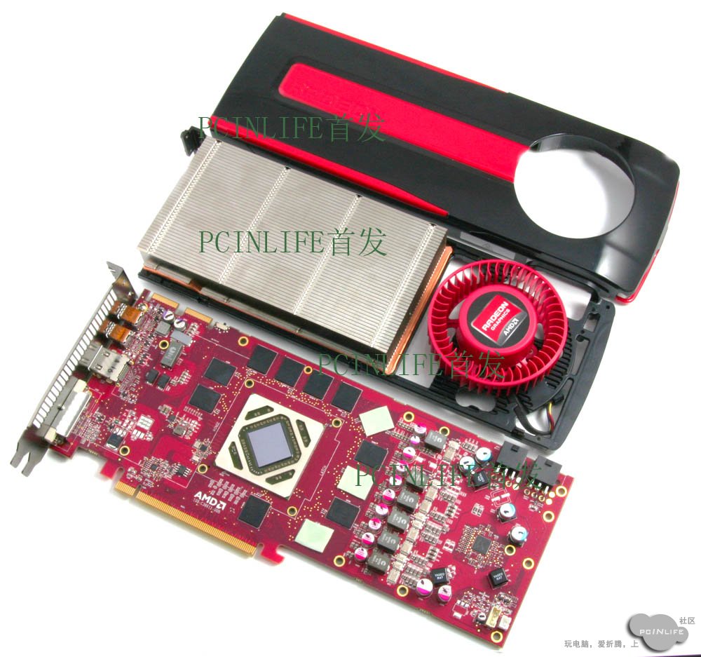
__________________
2013 UPCOMING PC-GAME |
|
2011-12-21, 06:46 PM
#8
|
|
|
Elite Member
  加入日期: Mar 2003 您的住址: Vancouver, Canada
文章: 15,006
|
現在都是那麼大一個散熱片麼
  |
|
2011-12-21, 07:00 PM
#9
|
|
|
Junior Member
加入日期: Jan 2003
文章: 967
|
引用:
光看圖片就口水流滿地啊~~~ 散熱器看來效能應該不錯,而且似乎對整張顯卡全配件(+Ram)散熱,加上出風口加大,溫度控制應該可以比上代更好。 唯一被取捨掉的就是沒有雙DVI了,舊的CRT+LCD會有點麻煩...希望DVI可以轉D-sub, HDMI轉DVI應該沒問題。 此文章於 2011-12-21 07:03 PM 被 ccyew 編輯. |
|
|
2011-12-21, 07:01 PM
#10
|
|


