引用:
|
作者weiter5494@2014-05-01, 04:11 PM #258
|
是虎是豹,拉出來咬咬就知道!沉潛兩年,影武者Kabini/Temash退位,本尊Beema/Mullins現身。

AMD SoC diagram

AMD Mobility Roadmap

AMD以低功耗為訴求的微架構研發不及,為求2013年卡位,倉促以未完成品Jaguar急就章上場充數,一年後,完全體Puma+功成出關,力戰Intel低功耗版Haswell與Atom,其中Mullins SoC更是專對Tablet市場而來。
在已完成的Jaguar主架構上,AMD過去一年內最終成功成功建置入過去未完成的瞬間智慧超頻(Intelligent Boost)技術與PSP(Platform Security Processor)硬體保全功能,佐以更優化的28nm製程,精煉出Puma+微架構。
Puma+ is based on the
same micro architecture as Jaguar, a 2-wide OoO design with the same number of execution units and data structures inside the chip. The memory interface remains unchanged as well at 64-bits wide. These new SoCs are still built on the same 28nm process as their predecessor. The process however has seen some improvements. Not only are both the CPU and GPU designs slightly better optimized for lower power operation, but both benefit from
improvements to the manufacturing process resulting in substantial decreases in leakage current.
為求更低的功耗,Beema/Mullins毅然放棄前代對多種DRAM模組的支援彈性,加強限制,且依然未支援在手機蔚為主流的AP+DRAM的PoP封裝。
Beema and Mullins platforms now ship with
more strict guidelines as to what sort of memory can be used on board and how traces must be routed. The result is a memory interface that shaves off more than
500mW when in this more strict, low power mode. OEMs looking to ship a design with socketed DRAM can still run the memory interface in a higher power mode to ensure memory compatibility. Beema/Mullins also show up to a
200mW reduction in power consumed by the display interface compared to Kabini/Temash.
Beema and Mullins are definitely in a good place, however they still do
consume more power at idle than the smartphone SoCs we typically find in iOS and Android tablets.
師法Intel作風(其實其他業者的Mobile SoC亦然),AMD現在也提供如汽車引擎般在短時間內提高轉速來換取更高扭力以加速的Turbo模式 - Intelligent Boost。
Beema and Mullins SoCs can
take advantage of available thermal headroom to increase their maximum frequency for a limited period of time.
Similar to what Intel discovered in architecting its Bay Trail silicon, the fact that in ultra portable form factors
it would run into a chassis temperature limit before it ever reached the maximum operating temperature of its silicon, AMD hit significantly higher frequencies without a substantial architecture change or new process node by
raising the max thermal operating point of the silicon.
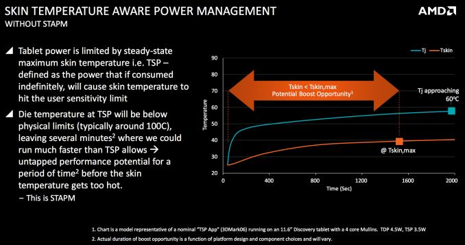
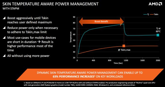
顧及機殼表面溫度影響所及的所用戶體驗,可耐熱至100°C的晶片核心,AMD在達60°C時便開始對CPU/GPU鎖頻。其實在100°C的物理極限內作短時間的超頻既不使機殼溫度長時間過度飆升,也不傷及SoC本身,何樂而不為?這就是STAPM(Skin Temperature Aware Power Management)節能技術。神奇之處是這項技術毋須系統廠在硬體上添加額外的溫測器。
What really matters isn’t if the silicon is running warm but rather
if the chassis is running too warm. With Beema and Mullins, AMD increases the silicon temperature limit to around 100°C (
still within physical limits) but instead relies on the surface temperature of the device to determine when to throttle back the CPU/GPU. In AMD’s own words, this allows the SoC
to run at a much higher frequency for up to several minutes before having to scale back down. Without requiring any additional sensors or hardware from the OEM, what AMD does instead is gives the OEM tools to properly map SoC temperature to chassis skin temperature.


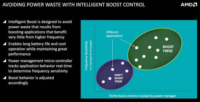
AMD宣稱,其Intelligent Boost可自行判斷超頻的時機,不浪費不必要的功耗。
The updated power management unit looks at
the response to frequency scaling of a given workload and will only boost when the workload will actually benefit from being boosted. This evaluation happens
at the hardware instruction level and not at the OS/software layer.

2012年向ARM授權Cortex-A5的AMD,雖然隔年便在其Kabini/Temash中植入,因為相關軟體未及時就緒而任其沉眠,直至今日終於有能力將其喚醒,抗衡Intel TXT(Trusted Execution Technology)。


叫板Bay Trail-T,Mullins效能來勢洶洶。

AMD處理器功耗遷移沿革

好戲在後頭,AMD技術水平向Intel靠攏,壓箱寶即將盡出,能一搏Intel嗎?